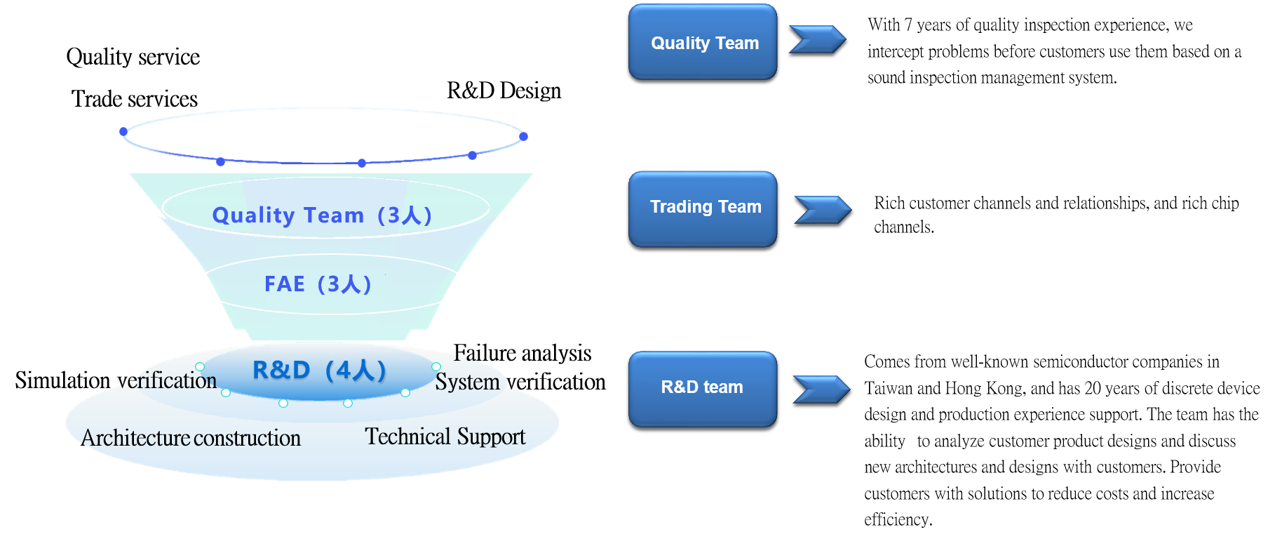
公司拥有20年分立器件和集成电路芯片的设计经验,团队来自中国、台湾、香港等地的知名半导体企业,具备丰富的分析能力和设计创新能力,能根据客户需求提供降本增效的方案。 Comes from well-known semiconductor companies in Taiwan and Hong Kong, and has 20 years of discrete device design and production experience support. The team has the ability to analyze customer product designs and discuss new architectures and designs with customers. Provide customers with solutions to reduce costs and increase efficiency.
设计与开发资源R&D Design
整合全球领先的设计资源,包括伯恩半导体与研究所合作,支持半导体前端晶圆制造工艺和后端封测技术,并拥有自制治具的能力,能够提供应用电路板(电源板、主板等)的全方位设计开发支持。 Integrate the design resources of Bern Semiconductor and the research institute to carry out project research and development; Capable of semiconductor front-end wafer manufacturing process, back-end packaging and testing technology, and self-made fixture; 20 years of experience in discrete device and integrated circuit chip design; And the design and development support capabilities for application circuit boards (power boards, circuit boards, motherboards) and other supporting components.
核心技术开发Core development
研发范围涵盖高功率器件和超结MOS设计,计划未来进一步拓展至高压电源管理芯片的开发,增强自主品牌芯片产品的竞争力。 The scope of research and development covers high-power devices and super-junction MOS design, and it is planned to further expand to the development of high-voltage power management chips in the future to enhance the competitiveness of independent brand chip products.
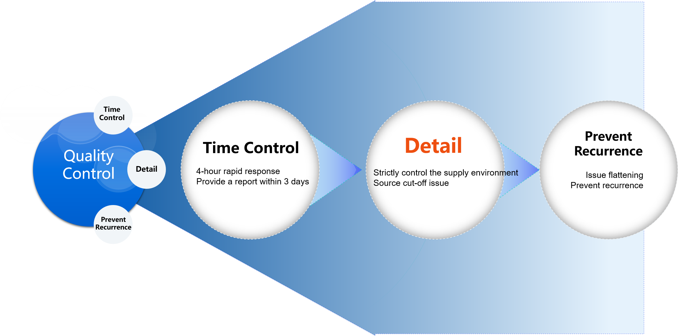
品质控制流程Quality control process
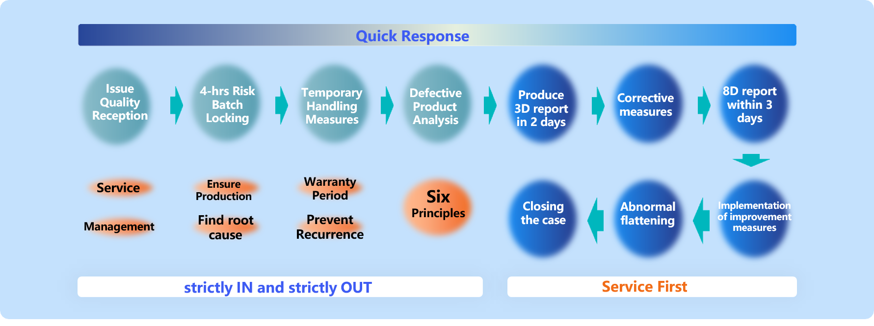
快速响应机制Quick Response
4小时内风险批次锁定,保证快速处理异常,最大化减少质量问题的影响。 Risk batches are locked within 4 hours to ensure rapid processing of exceptions and minimize the impact of quality problems.
异常处理流程Exception handling process
3D报告:2天内生成3D报告,详细分析不良原因并给出改善建议。 Produce 3D report in 2 days
8D报告:3天内提交8D报告,提供全面的纠正和预防措施,防止质量问题再度发生。 8D report within 3 days
全程质量监控Whole process quality control
从材料、生产到出货的全程监控,以确保芯片品质的高标准。 Monitor the entire process from materials, production to shipment to ensure high standards of chip quality.
异常处理能力Issue Handling Capability
我司拥有业界专业的团队,集电路设计,工厂生产、上游晶圆于一体,晶圆→封装测试可实现从生产源头把控品质。 Our company has a professional team in the industry, integrating circuit design, factory production, and upstream wafer manufacturing. Wafer packaging testing can achieve quality control from the production source.
我司FAE、原厂技术人员可第一时间到场解决各种突发问题,以专业、严谨的态度为客户生产保驾护航! Our FAE and original technical personnel can be on site to solve various unexpected problems in the first time and provide professional and rigorous support for customer production!
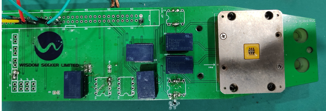
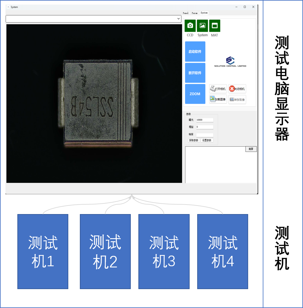
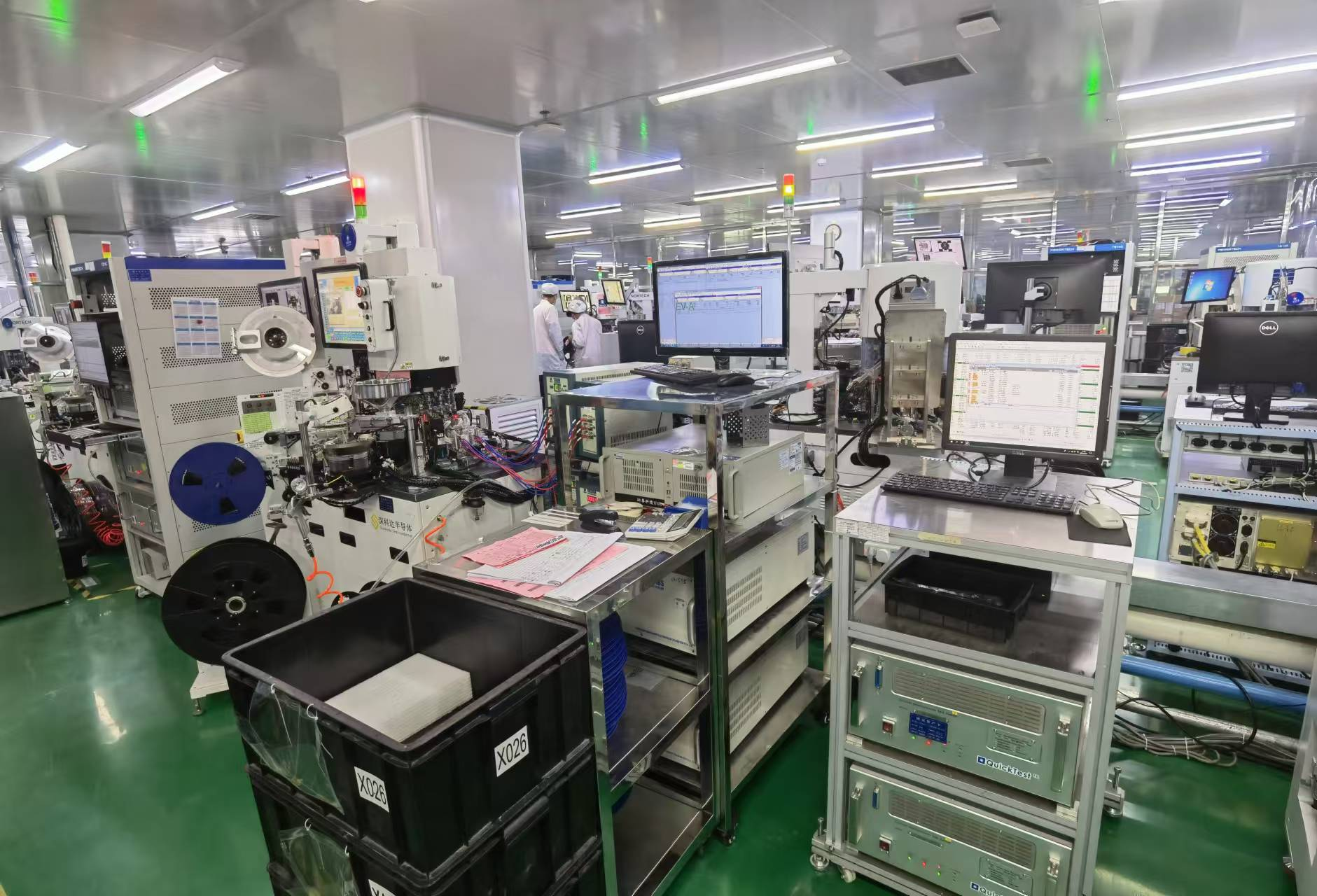
芯片最终测试能力Final testing capability of chip
先进FAB工厂支持Advanced FAB factory support
与国内外知名FAB工厂合作,支持分立器件加工,缩短晶圆交期,确保交货效率和质量。 Cooperate with well-known FAB factories at home and abroad to support discrete device processing, shorten wafer delivery time, and ensure delivery efficiency and quality.
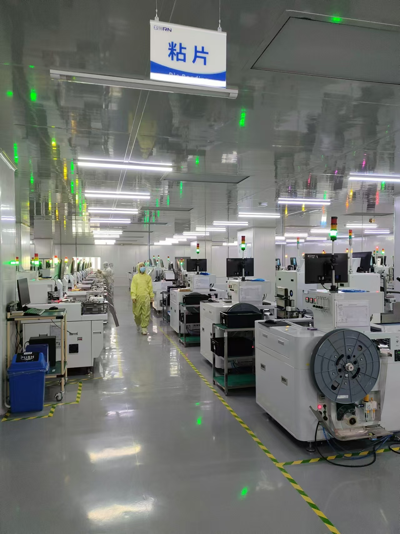
专业封测厂服务Professional packaging and testing factory services
提供高质量封装检测服务,严控封装过程,确保产品在出厂前的高可靠性和一致性,满足多种行业需求。 Provide high-quality packaging testing services, strictly control the packaging process, ensure high reliability and consistency of products before leaving the factory, and meet the needs of various industries.
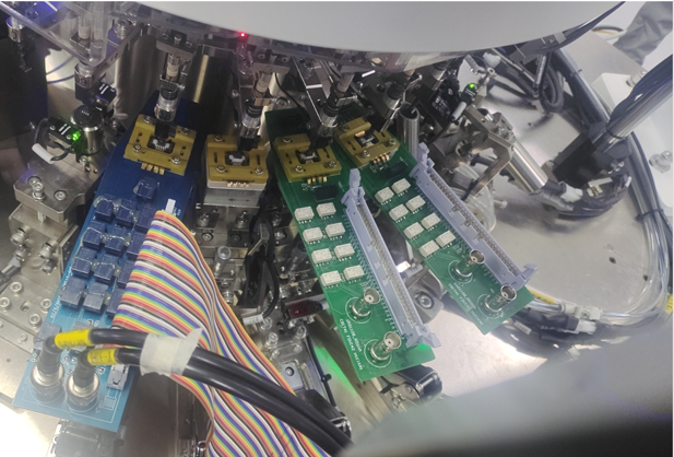
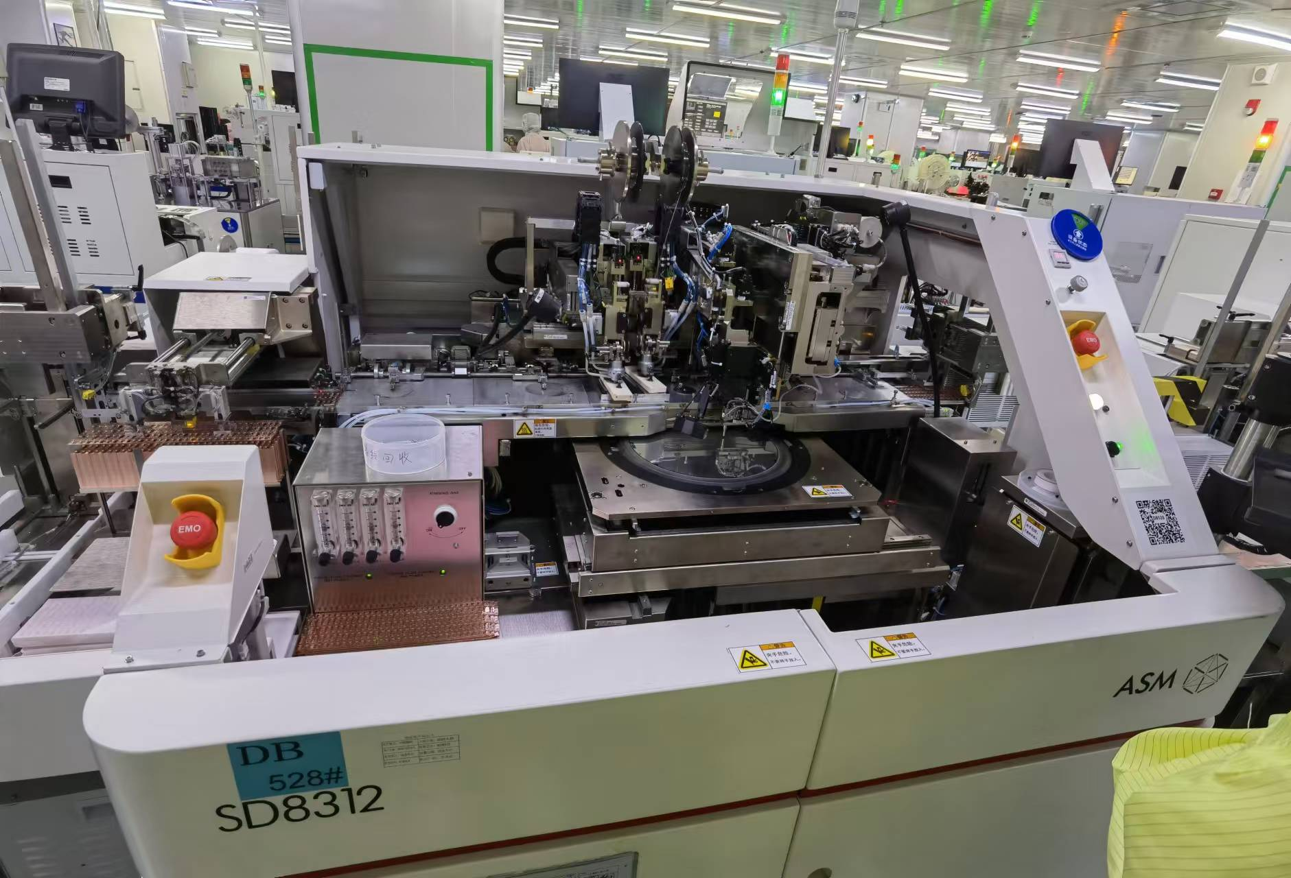
测试转盘实物图Physical picture of test turntable
战略合作方Strategic Partner
我们的合作伙伴包括多家领先的晶圆製造厂及封测厂,这些企业在全球半导体产业中具备举足轻重的地位。它们不仅拥有先进的製程技术与核心竞争优势,还在世界各地建立了广泛的市场影响力与稳定的客户基础。透过这些伙伴的技术支持与製造能力,我们能够共同推动产业创新,满足多元化市场需求,并实现全球市场的高效佈局与拓展。 Our partners include a number of leading wafer manufacturing plants and packaging and testing plants, which play a pivotal role in the global semiconductor industry. Not only do they possess advanced process technology and core competitive advantages, they have also established extensive market influence and a stable customer base around the world. Through the technical support and manufacturing capabilities of these partners, we can jointly promote industrial innovation, meet diversified market needs, and achieve efficient layout and expansion of the global market.
晶圆wafer
国内外先进的FAB厂,丰富的分立器件加工经验,缩短晶圆交期,提高交货效率Advanced FAB factories at home and abroad, rich experience in discrete device processing, shorten wafer delivery time, and improve delivery efficiency.
封测closed beta
国内外一线封测厂,从源头严格把控产品封装质量,给客户提供稳定可靠的产品First tier packaging and testing factories both domestically and internationally strictly control the quality of product packaging from the source, providing customers with stable and reliable products.
未来规划Future planning
产线投资与扩展Production line investment and expansion
计划在未来投资建设小封装产线,进一步优化封装成本,并提升产品的交付效率,为客户提供更具竞争力的芯片解决方案。 We plan to invest in the construction of small packaging production lines in the future to further optimize packaging costs, improve product delivery efficiency, and provide customers with more competitive chip solutions.
创新产品研发Innovative product development
将持续发展自主品牌和新型高功率芯片,以扩大产品种类和应用领域,积极布局新能源、物联网等新兴市场,推动技术创新并满足市场的多样化需求。 We will continue to develop independent brands and new high-power chips to expand product categories and application areas, actively deploy emerging markets such as new energy and the Internet of Things, promote technological innovation, and meet the diverse needs of the market.
质量管理理念Quality management concept
全程控制:从设计、材料采购到生产和出货进行全程品质监控,确保产品达到国际标准。 Full-process control: Full-process quality control from design, material procurement to production and shipment to ensure that products meet international standards.
客户为先:我们承诺为客户提供符合要求的高品质芯片,以客户需求为导向,推动产品持续改进。 Customer first: We are committed to providing customers with high-quality chips that meet their requirements, and are guided by customer needs to promote continuous product improvement.
持续改进:公司内部通过持续培训和技术改进,推动质量管理体系的优化,以保持在半导体行业中的质量竞争优势。 Continuous improvement: The company promotes the optimization of the quality management system through continuous training and technical improvement to maintain quality competitiveness in the semiconductor industry.